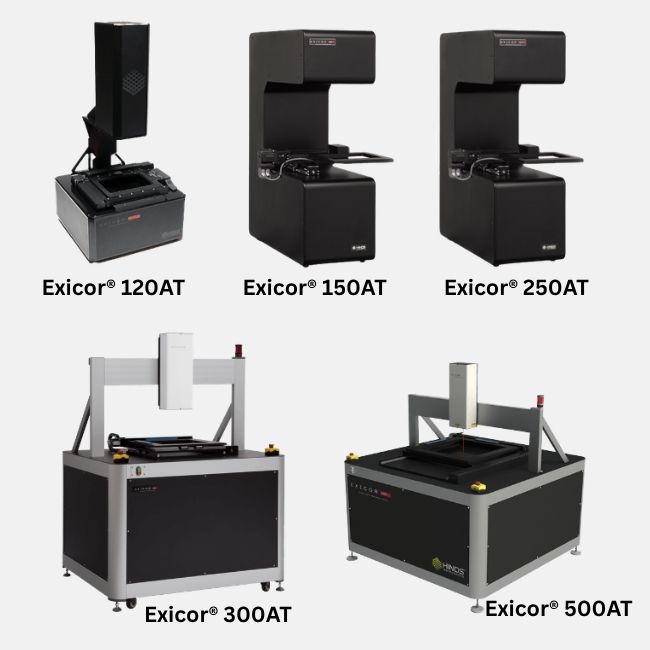
The Exicor® Series of birefringence metrology systems delivers industry‑leading sensitivity and repeatability for low‑level birefringence measurement across optical materials, consumer electronics, and semiconductor manufacturing.
Designed to support both quality control and advanced inspection, the Exicor® platform enables accurate, full‑field birefringence analysis in applications ranging from plastic films, lens blanks, laser crystals, and display glass to silicon and silicon carbide (SiC) wafer inspection and photomask quality assessment.
With automated, high‑resolution mapping and proven performance in production and R&D environments, the Exicor® Series provides reliable insight into stress‑induced optical effects, material uniformity, and process stability critical to modern optical and microelectronics manufacturing.
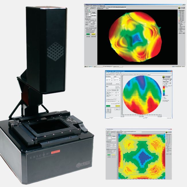
The Exicor® AT delivers advanced birefringence metrology through a combination of high speed, precision, and operational simplicity. Its standard Scan in Motion™ (SIM) package enables practical high‑spatial‑resolution scanning with grid spacing below 1 mm, while offering unprecedented sensitivity for low‑level birefringence measurement. The system simultaneously measures birefringence magnitude and angle, providing highly repeatable, high‑speed results through fully automatic mapping.
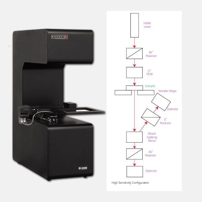
With no moving optics, the Exicor® AT ensures consistent measurements by eliminating the need for continual stage or sample adjustments. Guided by intuitive, user‑friendly software, the system streamlines testing, data collection, and analysis, making it ideally suited for semiconductor wafer inspection and photomask quality assessment in both production and research environments.
120AT | All Other AT Models | |
Retardation Range: | 0.005 to 300+ nm | 0.005 to 300+ nm |
Retardation Resolution / Repeatability1, 2: | 0.001 nm / ± 0.02 nm | 0.001 nm / ± 0.015 nm |
Angular Resolution / Repeatability1: | 0.01º / ± 0.07° | 0.01º / ± 0.07° |
Measurement Rate / Time3: | 15 samples/sec (at 1nm spacing) | up to 100 pps / sample size dependent |
Light Source Wavelength4: | Various (625nm standard) | Various (632.8 nm standard) |
Measurement Spot Diameter5: | Between 1 mm and 3 mm (can be as low as <50 µm) | Between 1 mm and 3 mm (can be as low as <50 µm) |
Modulation Technique / Frequency: | PEMLabsTM Photoelastic Modulator / 50 kHz and 50/60 kHz | PEMLabsTM Photoelastic Modulator / 50 kHz and 50/60 kHz |
Demodulation Analysis Technique: | Hinds Instruments SignalocTM Lock-in Amplifier | Hinds Instruments SignalocTM Lock-in Amplifier |
Measurement Units: | nm (retardation), ° (angle) | nm (retardation), ° (angle) |
The Exicor® platform from Hinds Insrtuments is designed to be highly adaptable, enabling custom configuration to meet the specific requirements of advanced birefringence measurement applications. Originally developed for nanometre‑range, industrialised birefringence measurement, Exicor systems were engineered in recognition that polarisation analysis—particularly birefringence measurement—is frequently driven by application‑specific and non‑standard requirements.
Many customer processes are proprietary in nature and require measurement solutions that can be adapted both quickly and cost‑effectively. To support this, Exicor systems utilise a modular architecture, incorporating configurable optical and electronic subsystems that can be assembled and tailored with minimal non‑recurring engineering (NRE) effort. This approach allows customised system configurations to be delivered efficiently, while maintaining proven performance and measurement reliability.
The Exicor product family includes over three dozen system models, a significant proportion of which represent custom or semi‑custom configurations developed to address specific measurement challenges. This flexibility enables Exicor systems to support a wide range of research, development, and production environments where standard, off‑the‑shelf solutions may not be sufficient.
By combining modular system design with advanced polarisation and birefringence measurement technology, Exicor systems provide users with tailored measurement capability—supporting improved process control, enhanced product performance, and increased competitiveness in precision optics and advanced materials markets.
The Exicor® 120AT is designed for quality control metrology and low‑level birefringence measurement across a wide range of optical and polymer materials. Its high sensitivity and repeatability make it an ideal solution for manufacturers and laboratories requiring reliable stress and optical uniformity analysis.
Plastic Films – Measures residual and process‑induced birefringence to support material uniformity, performance optimisation, and production consistency in film manufacturing.
Lens Blanks – Detects internal stress and birefringence non‑uniformities prior to polishing and finishing, helping improve optical quality and reduce downstream rejects.
Laser Crystals – Quantifies low‑level birefringence that can impact beam quality and laser performance, supporting crystal selection and process optimisation.
Cell Phone Display Windows – Evaluates stress‑induced birefringence in glass and cover materials used in mobile and consumer electronics, helping maintain display clarity and optical performance.
The Exicor® 120AT is widely used in optical manufacturing, materials research, and production quality assurance, where accurate, repeatable birefringence data is essential.
The Exicor® 150AT is purpose‑built for advanced semiconductor and microelectronics inspection, delivering high‑resolution, full‑field birefringence measurements for critical process control and material integrity analysis.
The Exicor® 150AT performs full‑field birefringence distribution measurements on:
It accurately identifies stress‑induced birefringence resulting from processes such as cutting, grinding, polishing, and epitaxial growth. This enables manufacturers to assess crystal lattice integrity, monitor process stability, and support yield improvement in power electronics, MEMS, and advanced semiconductor devices.
The system conducts high‑resolution birefringence uniformity scans on all photomask types, helping detect optical distortions caused by:
By identifying birefringence‑related deviations early, the Exicor® 150AT supports improved photolithographic pattern accuracy and consistent pattern transfer in advanced semiconductor manufacturing.
Thanks for getting in touch!
Our team will respond as soon as possible.
Product Enquiry
Please complete all fields