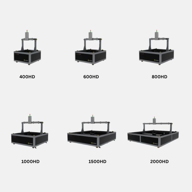
The Exicor® HD Series is a high‑stability, automated birefringence measurement system designed for semiconductor wafer inspection and photomask testing. Built on the proven low‑level birefringence measurement technology of the Exicor core, the system combines precision automated motion control with intuitive scanning software to enable repeatable, routine evaluation of semiconductor wafers and photomasks.
The Exicor® HD Series is a newly engineered, heavy‑duty birefringence measurement platform designed to support large‑format and high‑mass sample inspection with exceptional stability and precision. Built around precision automated motion control and a rigid all‑steel base, the Exicor® HD provides a robust and reliable solution for demanding measurement environments. The system offers a high degree of configurability, including flexible system sizes, maximum sample capacities, selectable wavelengths, and customizable software options, allowing the platform to be tailored to specific application and sample requirements. The Exicor® HD Series scales seamlessly across multiple models to accommodate a wide range of sample dimensions and load capacities.
| Model | System Size (X × Y × Z, mm) | Max. Sample Size (X × Y × Z, mm) | Max. Load (lbs / kg) |
|---|---|---|---|
| Exicor® 400HD | 1265 × 1414 × 2050 | 400 × 400 × 400 | 450 / 205 |
| Exicor® 600HD | 1465 × 1614 × 2050 | 600 × 600 × 500 | 1,100 / 500 |
| Exicor® 800HD | 1663 × 1814 × 2050 | 800 × 800 × 500 | 1,910 / 865 |
| Exicor® 1000HD | 1865 × 2014 × 2050 | 1000 × 1000 × 500 | 2,910 / 1,320 |
| Exicor® 1500HD | 2366 × 2662 × 2050 | 1500 × 1500 × 500 | 6,600 / 3,000 |
| Exicor® 2000HD | 2790 × 3162 × 2050 | 2000 × 2000 × 500 | 11,750 / 5,400 |
Designed for performance, scalability, and long‑term measurement stability, the Exicor® HD Series meets the needs of advanced inspection workflows requiring large sample handling, precise motion control, and configurable system architecture.
| Retardation Range: | 0.005 to 300+ nm | |
| Retardation Resolution / Repeatability1, 2: | 0.001 nm / ± 0.015 nm | |
| Angular Resolution / Repeatability1: | 0.01º / ± 0.07º | |
| Measurement Rate / Time3: | up to 100 pps / sample size dependent | |
| Light Source Wavelength4: | Various (632.8 nm standard) | |
| Measurement Spot Diameter5: | Between 1mm & 3mm native (can be as low as <50 µm) | |
| Modulation Technique: | PEMLabsTM Photoelastic Modulator | |
| Measurement Units: | nm (retardation),º (angle) | |
| Loading Options: | Front and Overhead Options | |
The Exicor® platform from Hinds Insrtuments is designed to be highly adaptable, enabling custom configuration to meet the specific requirements of advanced birefringence measurement applications. Originally developed for nanometre‑range, industrialised birefringence measurement, Exicor systems were engineered in recognition that polarisation analysis—particularly birefringence measurement—is frequently driven by application‑specific and non‑standard requirements.
Many customer processes are proprietary in nature and require measurement solutions that can be adapted both quickly and cost‑effectively. To support this, Exicor systems utilise a modular architecture, incorporating configurable optical and electronic subsystems that can be assembled and tailored with minimal non‑recurring engineering (NRE) effort. This approach allows customised system configurations to be delivered efficiently, while maintaining proven performance and measurement reliability.
The Exicor product family includes over three dozen system models, a significant proportion of which represent custom or semi‑custom configurations developed to address specific measurement challenges. This flexibility enables Exicor systems to support a wide range of research, development, and production environments where standard, off‑the‑shelf solutions may not be sufficient.
By combining modular system design with advanced polarisation and birefringence measurement technology, Exicor systems provide users with tailored measurement capability—supporting improved process control, enhanced product performance, and increased competitiveness in precision optics and advanced materials markets.
The system enables full‑field birefringence distribution measurement on silicon and silicon carbide (SiC) wafers, supporting advanced semiconductor inspection and process control. It accurately identifies stress‑induced birefringence introduced during manufacturing steps such as cutting, grinding, polishing, and epitaxial growth, providing critical insight into crystal lattice integrity, material quality, and process stability.
High‑resolution birefringence uniformity scans are performed on photomasks of all types, allowing precise detection of optical performance deviations caused by material defects or processing‑related stress. This supports improved photolithographic pattern transfer accuracy, yield optimisation, and reliable performance in semiconductor manufacturing environments.
Thanks for getting in touch!
Our team will respond as soon as possible.
Product Enquiry
Please complete all fields